 Hi, I'm Tobi, online I usually go by as
 girst.
I'm based in Innsbruck, where by day I work as a network engineer, taking care of everything from our in-house data centres with a 100 gigabit backbone, to a distributed access network, spanning all over the beautiful state of Tyrol, to base services like DHCP, DNS, PKI, and much more.
All serious stuff; interesting and genuinely useful stuff.
So by night, I balance things out by hacking on electronics projects with zero practical applicability. If you came here to learn somehting - well, I hope you will, but I can promise you it will not ever be useful.
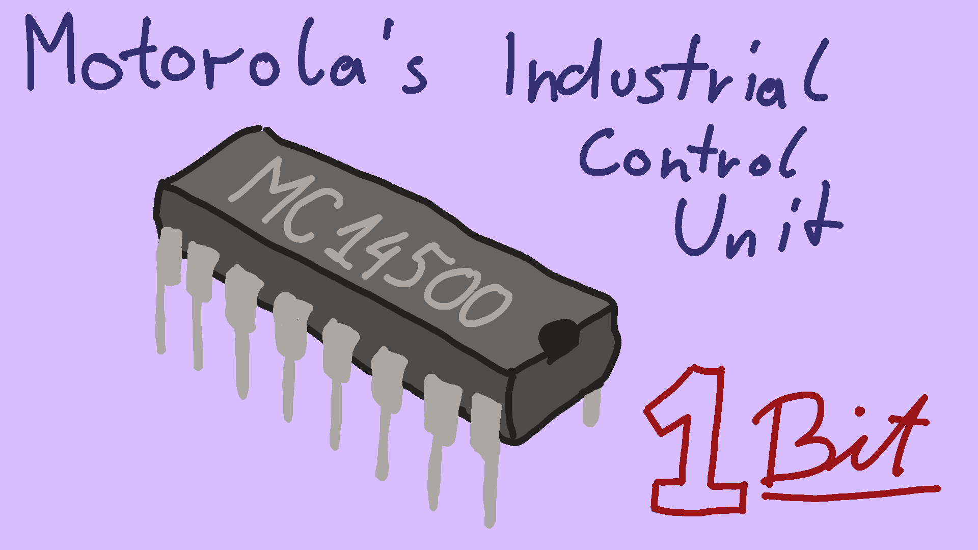
I've always had a bit of an obsession for tiny and/or obsolete microcontrollers. And today I want to tell you all about a long obsolete CPU, with a not 8, not 4, but 1-bit data bus: the Motorola MC14500.
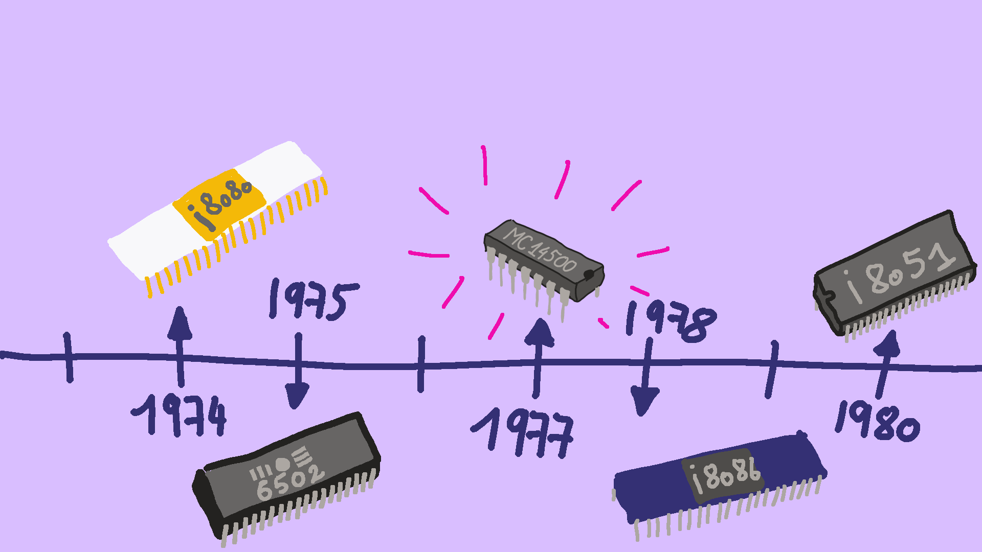
The MC14500 was released in 1977. For some context, that's right between the MOS 6502 and Intel 8086, which form the basis of the Commodore 64 and the IBM PC, respectively. It's also fairly close to the release of the 4004, the first ever commercial microprocessor.
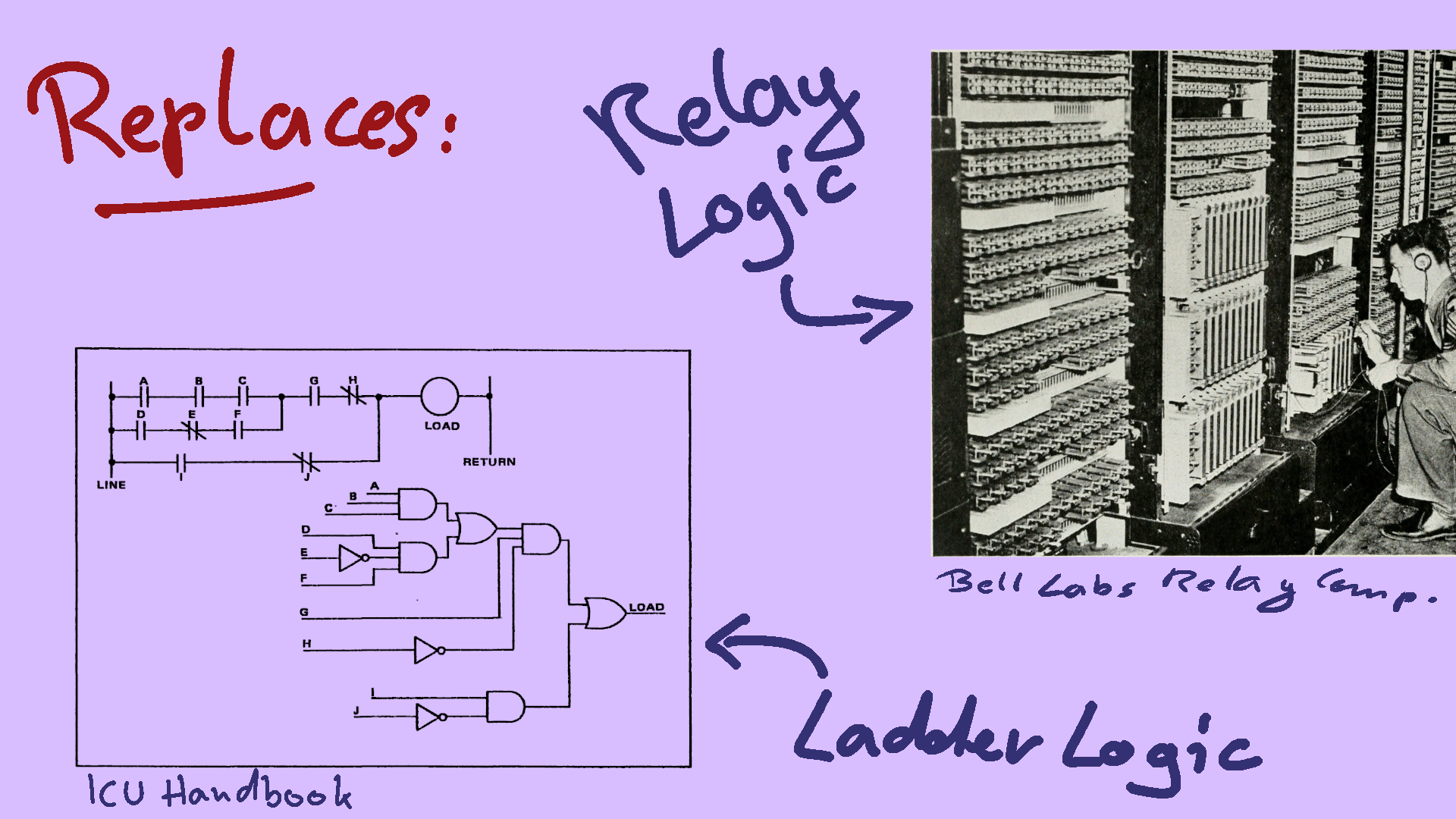
As you might imagine, the MC14500 doesn't play in the same league as most of the other processors on this slide. It was never designed to compete with them, though. Rather, the MC14500 was intended to replace logic circuits made out of electromechanical relays, for industrial control systems.
Part of what makes this chip so interesting to is is that it is so simple and cost-reduced, it can hardly be recognized as a CPU at all:
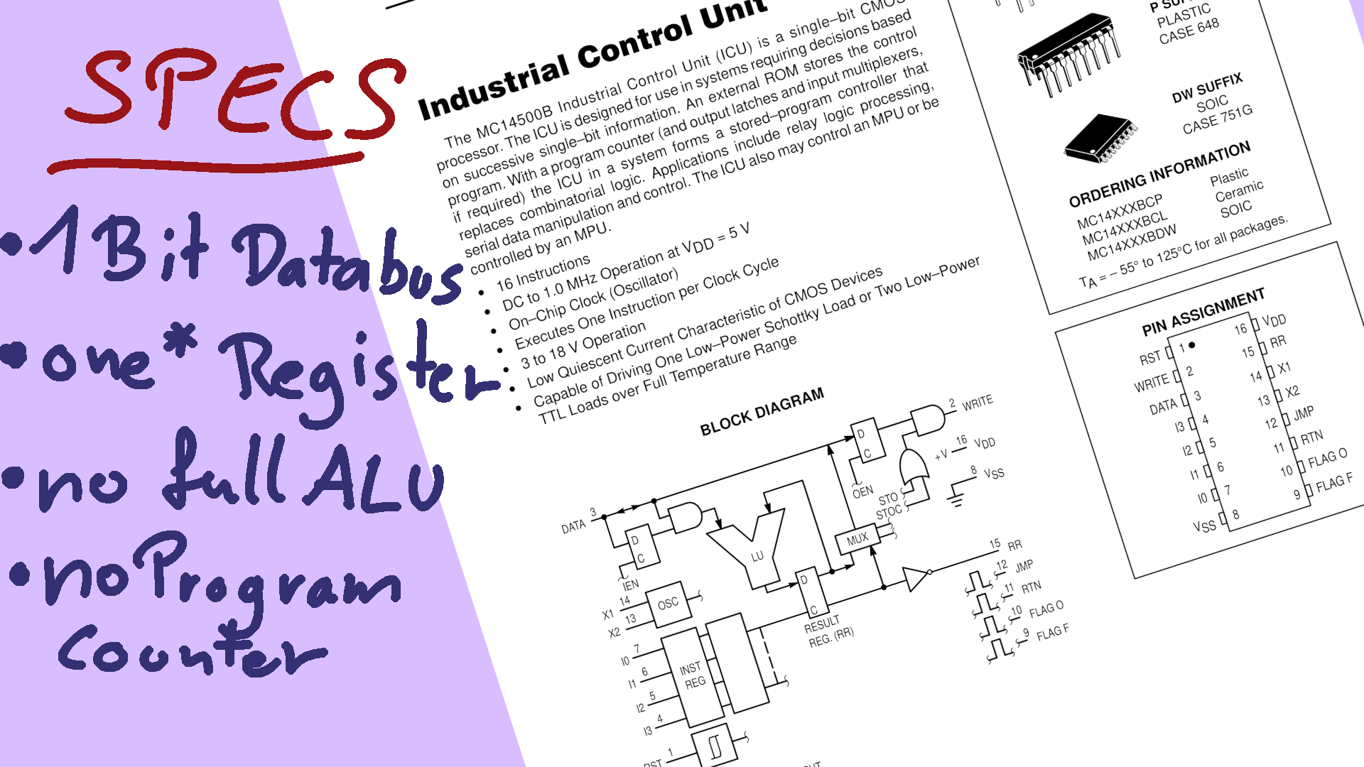
It's data bus is just a single bit wide, and unlike a bit-serial architecture, where multiple bits are processed in sequence and combined to form a larger machine word, this one truly operates on 1-bit words only.
The '14500 has just one register, called the Result Register. That was Motorola called the accumulator. All instructions that do logic operations take one parameter from the data bus, and modify the Result Register. Here's the first quirk I'll highlight: You can always see from the outside what the current state of the result register is. That's because there is an output pin directly connected to it. I'll get back to why that is later.
Some parts of what makes a CPU are just outright missing:
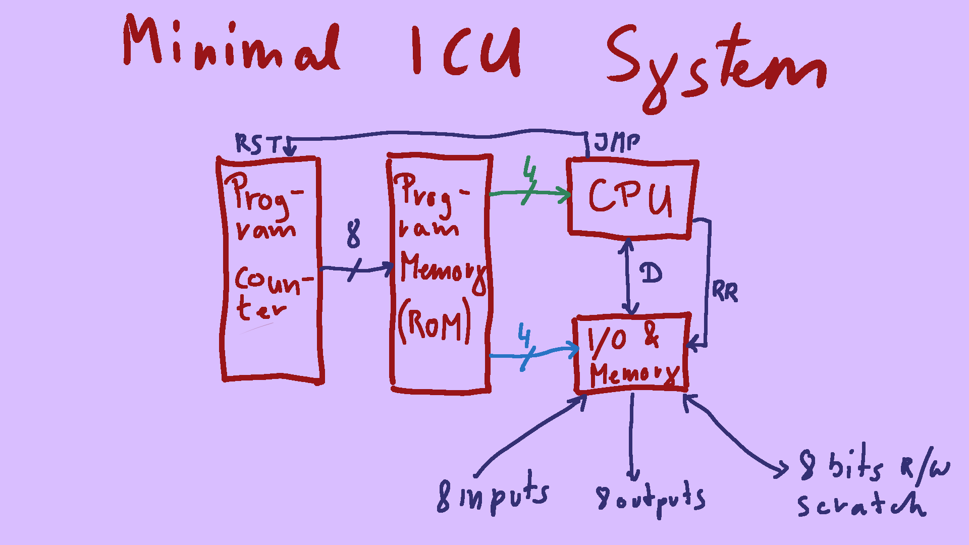
So, that has all been quite theoretical. So let's take a look at what Motorola calls "the minimal ICU system". A lot of what you see online today is essentially (modulo some flourishes) that minimal system. This includes the WDR-eins educational computer from the 1980ies, and the very recent PLC-14500 open hardware project. A PLC, short for programmable logic controller, is essentially an industrial Arduino. It's used to do exactly what the MC14500 was designed to do: automate industrial machinery. It has no control flow, the program simply executes each instruction read from a small RAM chip in sequence, until the program counter overflows, and then starts over. For peripherals, there usually are 8 inputs, 8 outputs, and 8 so-called scratch registers. The scratch registers are simply memory locations you can use to store variables, your RAM so to speak. The lower three bits of the address bus are hooked up to all three peripherals. The highest address bit then selects between the GPIO and the scratch registers. And to differentiate between inputs and outputs, the CPU's write signal is used. If you execute a STORE, it goes to the outputs, if you execute a LOAD it goes to the inputs. This way you essentially have read-only inputs, and write-only outputs.
We'll use this system for some very simple programming now.
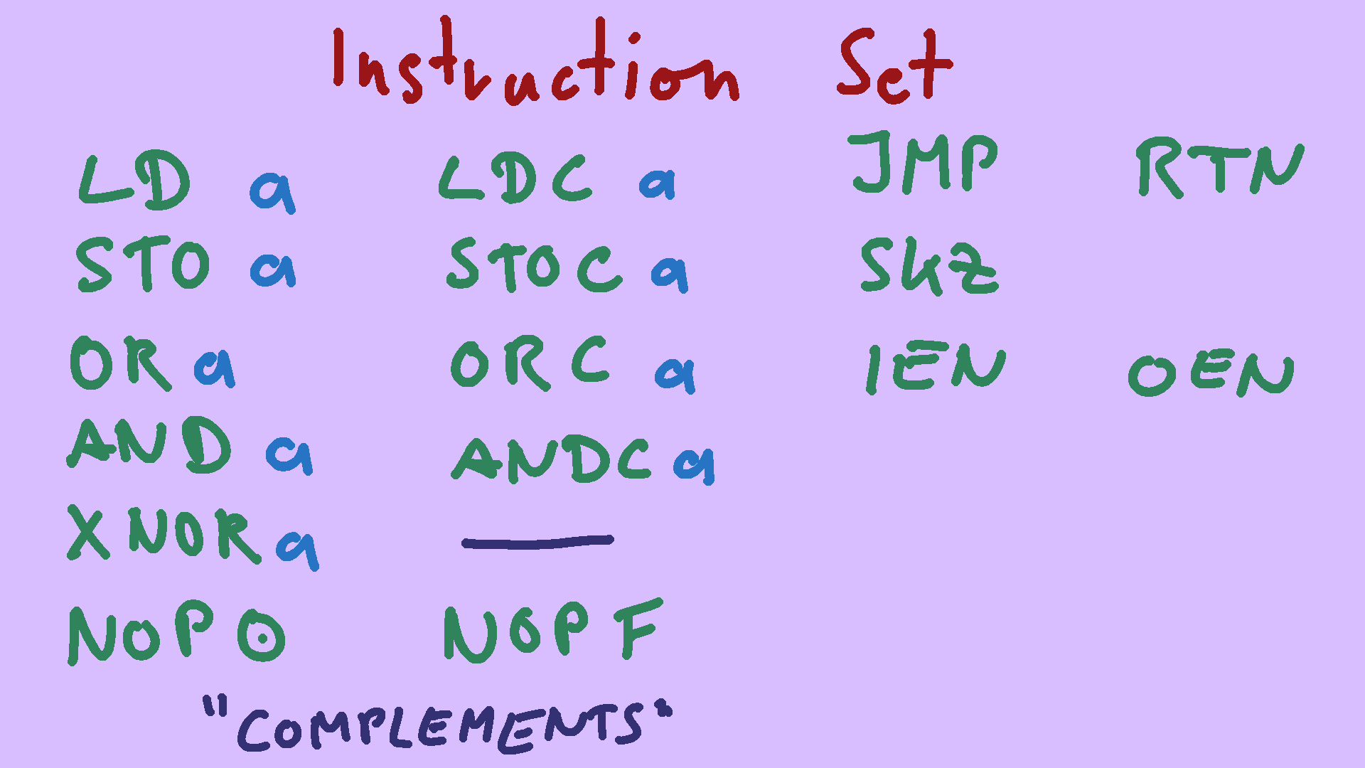
But first, let's take a quick look at the instruction set of the MC14500. It starts off pretty tame: there's LoaD, STOre, OR, AND. These do exactly what you'd expect from them: they all take one operand, and the other is implicitly the result register, i.e., the accumulator. Instead of XOR you get XNOR, the exclusive-NOR instruction, which is essentially an equality check. So far so good, but what is missing though is a NOT or INVERT instruction. Instead, most of these instructions come in pairs: For example, OR-Complement takes a bit from the data bus, inverts it, and then ORs it with the result register. This means that you'll have to rearrange your formulas quite a bit on paper until they can be implemented. deMorgan is your friend. then, there are JuMP, ReTurN, and SKip-if-Zero instructions for flow control; more on them later. IEN and OEN stand for Input-ENable and Output-ENable, they are an alternative way to do flow-control. Again, more on that later.
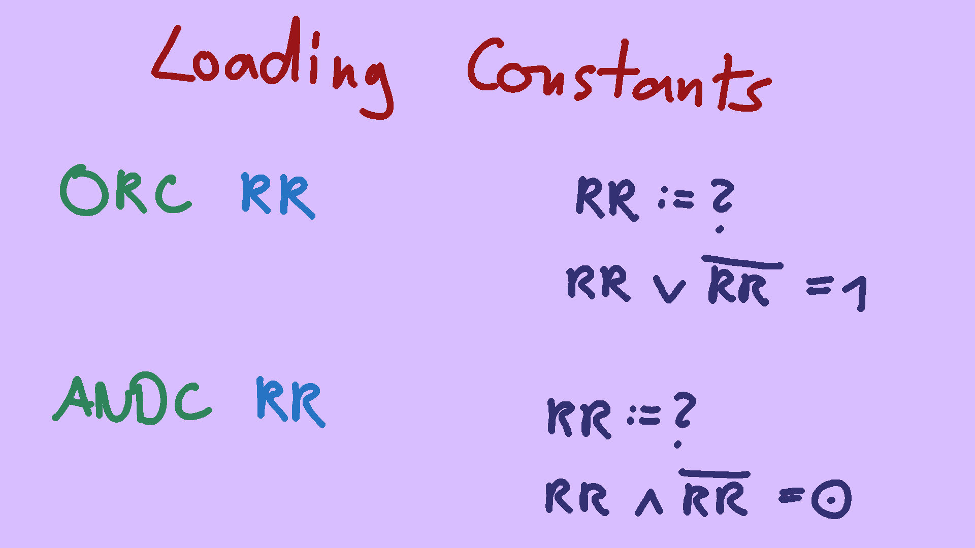
The LoaD instruction can only read from the data bus, there is no load-immediate variant of it available. So how do you load a constant? You could do what many modern architectures do and implement a zero-register with some logic gates. A zero register is a memory location that is read-only and always returns a known value, most of the time, zero. To load a constant one, you could use the LoaD-Complement of zero. But that wastes a precious memory location. You'll most likely have just sixteen addresses, and need every single one. And there is a better, more idiomatic, way. First of all, there are only two possible constants for a one-bit CPU: zero and one. If you take the logical OR of a random value and that value's inverse, you'll always get a one - independent of what was stored in RR beforehand. If RR contained a zero, we'd have zero OR one; if RR already stores a one, this does a one OR zero. We can apply a very similar trick to get a zero: take any random value, and AND it with its complement.
Let's talk about flow control.
 The MC14500 gives you not one, but two ways to control which part of your code is executed.
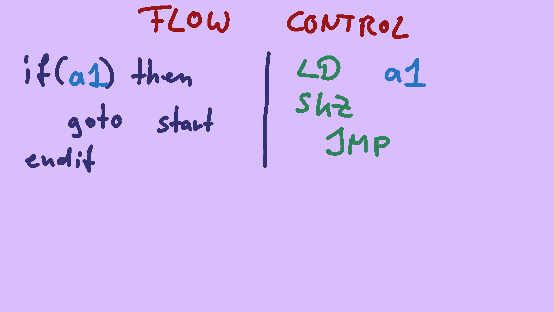
The first is called SKip-if-Zero.
This instruction simply looks at the Result Register, and if it contains a zero, the next instruction is turned into a no-op.
In this example, we look at some memory location, and if it contains a zero, we skip the jump, if it contains a one, we execute the jump.
Just as a reminder: the JuMP instruction simply strobes an output pin of the CPU - it could be hooked up to do whatever, but most commonly it simply resets the program counter and makes the program loop back to the beginning.
The MC14500 gives you not one, but two ways to control which part of your code is executed.
The first is called SKip-if-Zero.
This instruction simply looks at the Result Register, and if it contains a zero, the next instruction is turned into a no-op.
In this example, we look at some memory location, and if it contains a zero, we skip the jump, if it contains a one, we execute the jump.
Just as a reminder: the JuMP instruction simply strobes an output pin of the CPU - it could be hooked up to do whatever, but most commonly it simply resets the program counter and makes the program loop back to the beginning.
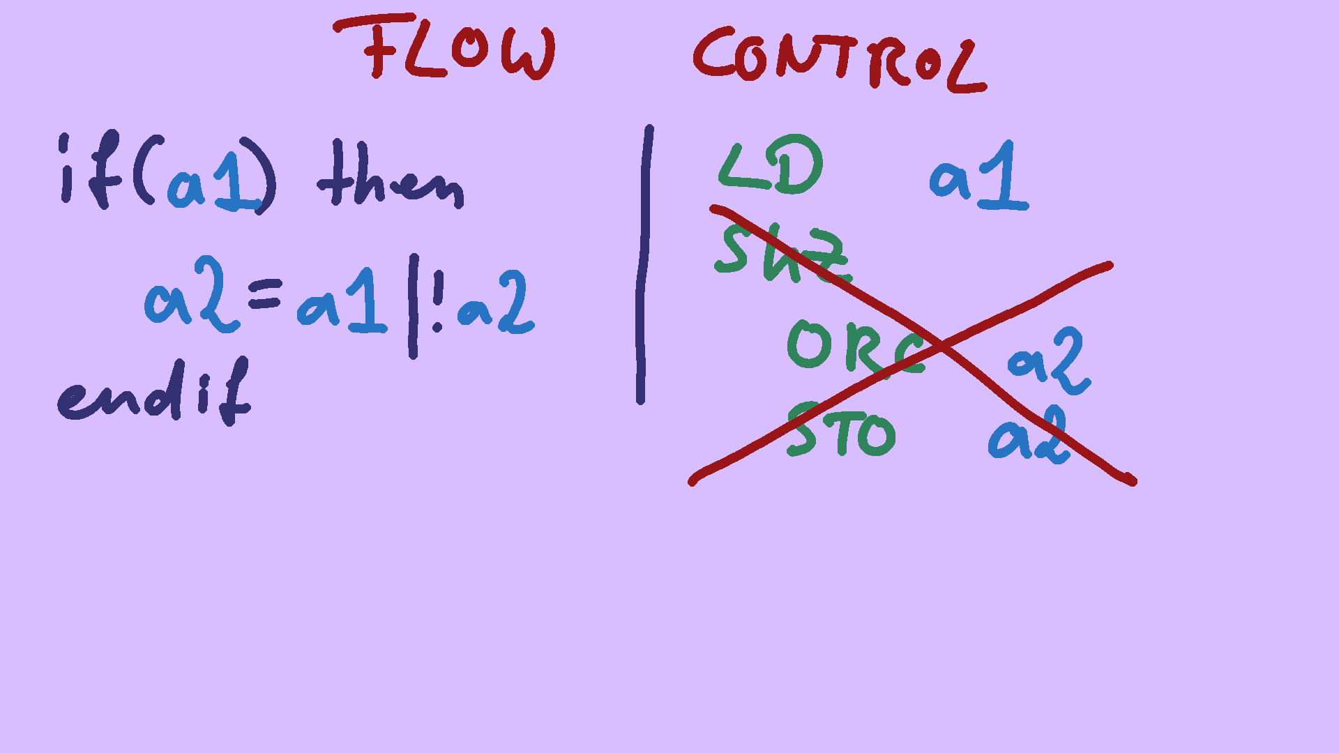
But if you want to skip more than one instruction, this gets tedous if not outright impossible. Take this example: if some_address is one, we want to load-modify-store other_address. This requires multiple instructions. And we can't place a SKip-if-Zero instruction in front of each, because we modify RR in between, which SKZ uses to determine when to skip.
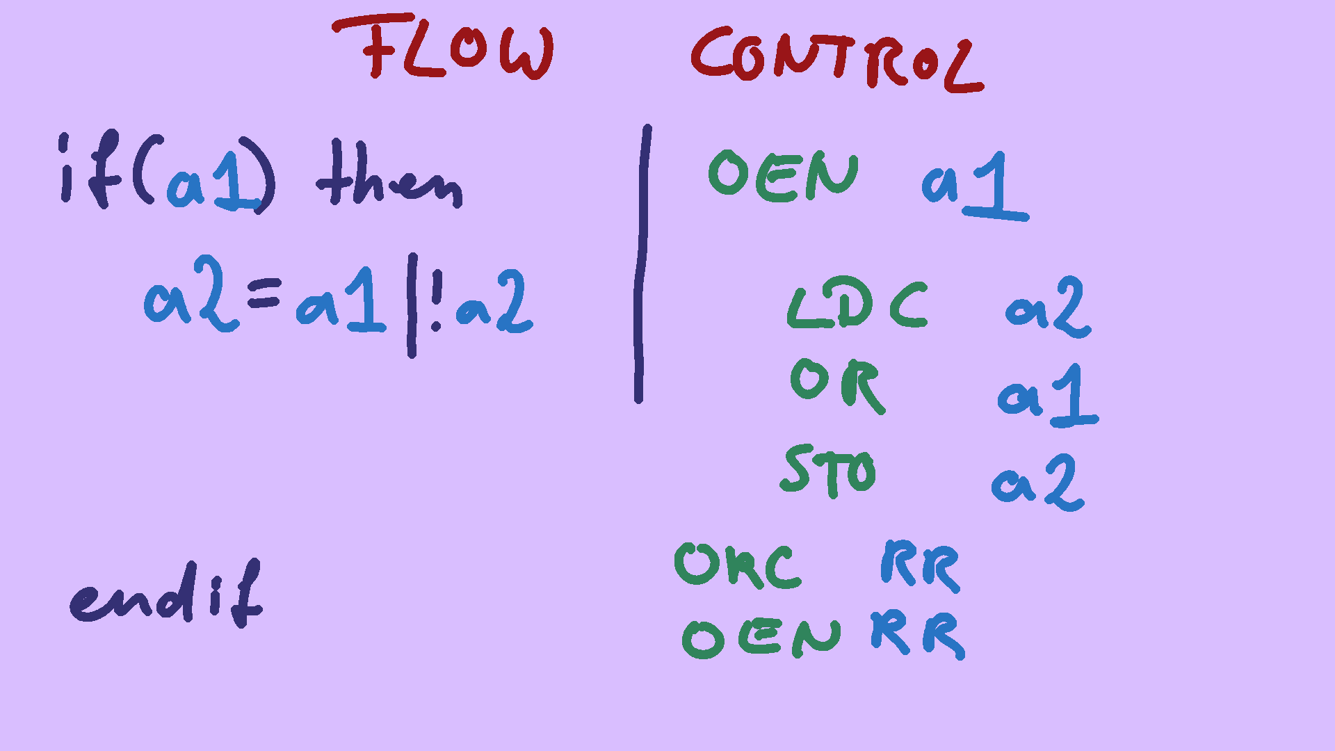 Instead, you'll have to make use of Input-ENable and Output-ENable in such a case.
If you disable the output, all STOre instructions get turned into no-ops.
If the input is disabled, all values on the data bus are replaced with zero - but we won't need that in this case.
So your program runs though the whole code, calculates a bunch of useless data, but never writes it back into RAM.
So it it essentially skipped.
That's essentially an if statement. The ORC RR and OEN RR is your endif: it forces a one into the result register, and enable output again unconditionally.
TODO: https://en.wikipedia.org/wiki/Ladder_logic#Industrial_STOP/START
Instead, you'll have to make use of Input-ENable and Output-ENable in such a case.
If you disable the output, all STOre instructions get turned into no-ops.
If the input is disabled, all values on the data bus are replaced with zero - but we won't need that in this case.
So your program runs though the whole code, calculates a bunch of useless data, but never writes it back into RAM.
So it it essentially skipped.
That's essentially an if statement. The ORC RR and OEN RR is your endif: it forces a one into the result register, and enable output again unconditionally.
TODO: https://en.wikipedia.org/wiki/Ladder_logic#Industrial_STOP/START
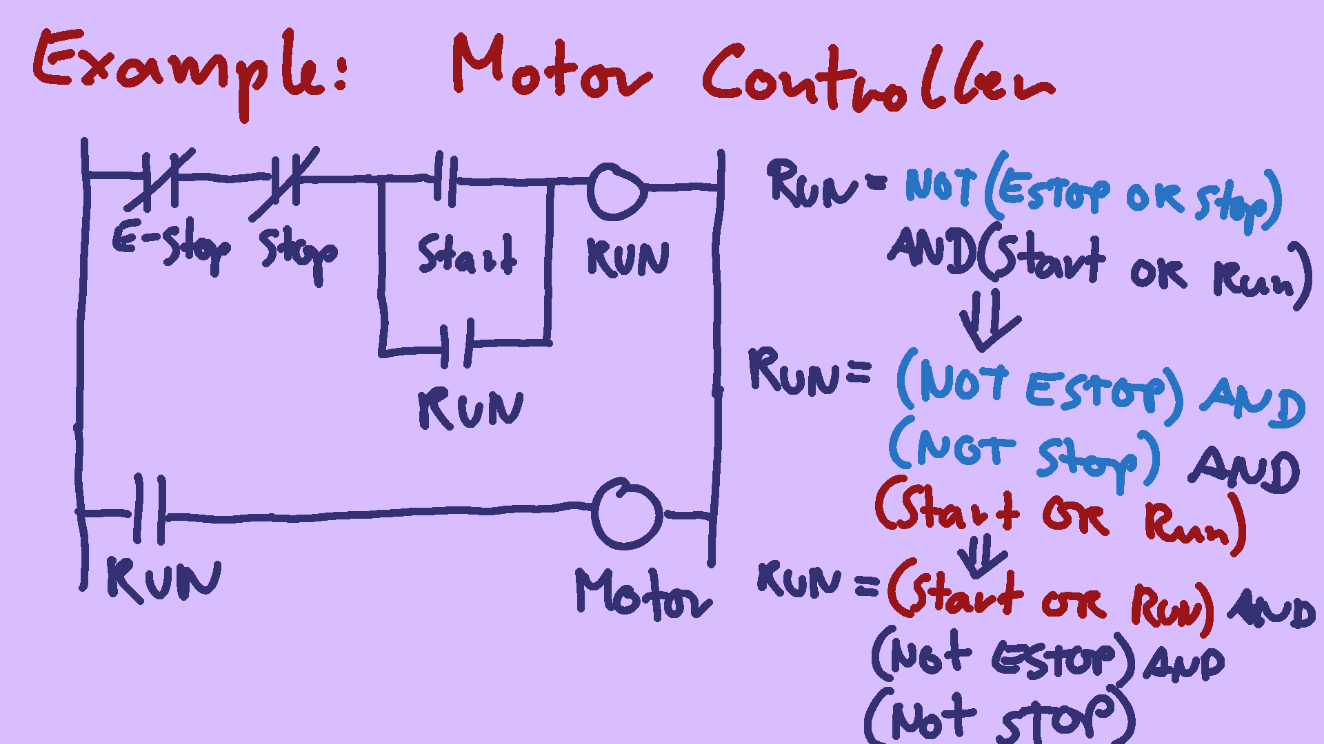
Finally, let's look at some realistic work. Let's say we want to create a motor controller for some industrial equipment. Since it's the nineteen-seventies, we've been given a ladder logic diagram of what our controller should do. Remember, this is exactly the use-case the 14500 was meant to replace. There is a normally-closed emergency stop button, a normally-closed regular stop button, and a normally open start button. if we press start, there is a complete connection from the source at the left, to the drain at the right, and the RUN signal gets turned on. The run signal also doubles as an additional input that keeps the circuit going once we let go of the run button. if we press the stop or e-stop button, the signal gets interrupted, and RUN turns back off, stopping our motor. you can think of that like the above equation is executed at every cycle through the program, which updates the RUN variable constantly.
For the actual equation, we need to do some re-arranging first. Since we don't have a NOT instruction, we need to get rid of it by applying deMorgan's law.
Having a NOT directly in front of a single variable is fine, because we can use for example LoaD-Complement or AND-Complement in these cases.
But we still need to get rid of the parentheses around Start-or-Run. Assembly programming is like using an old-school calculator: you have a runnning total, and can add one number to it, which updates the total. All we need to is to do this part first, and the parentheses go away by themselves.
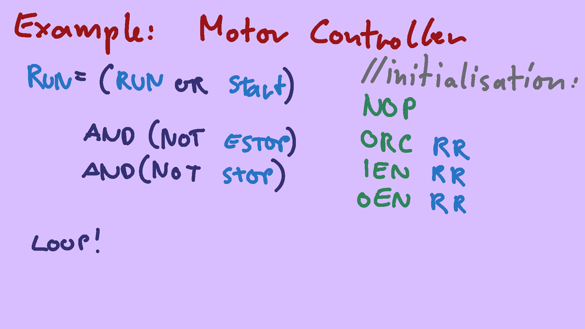
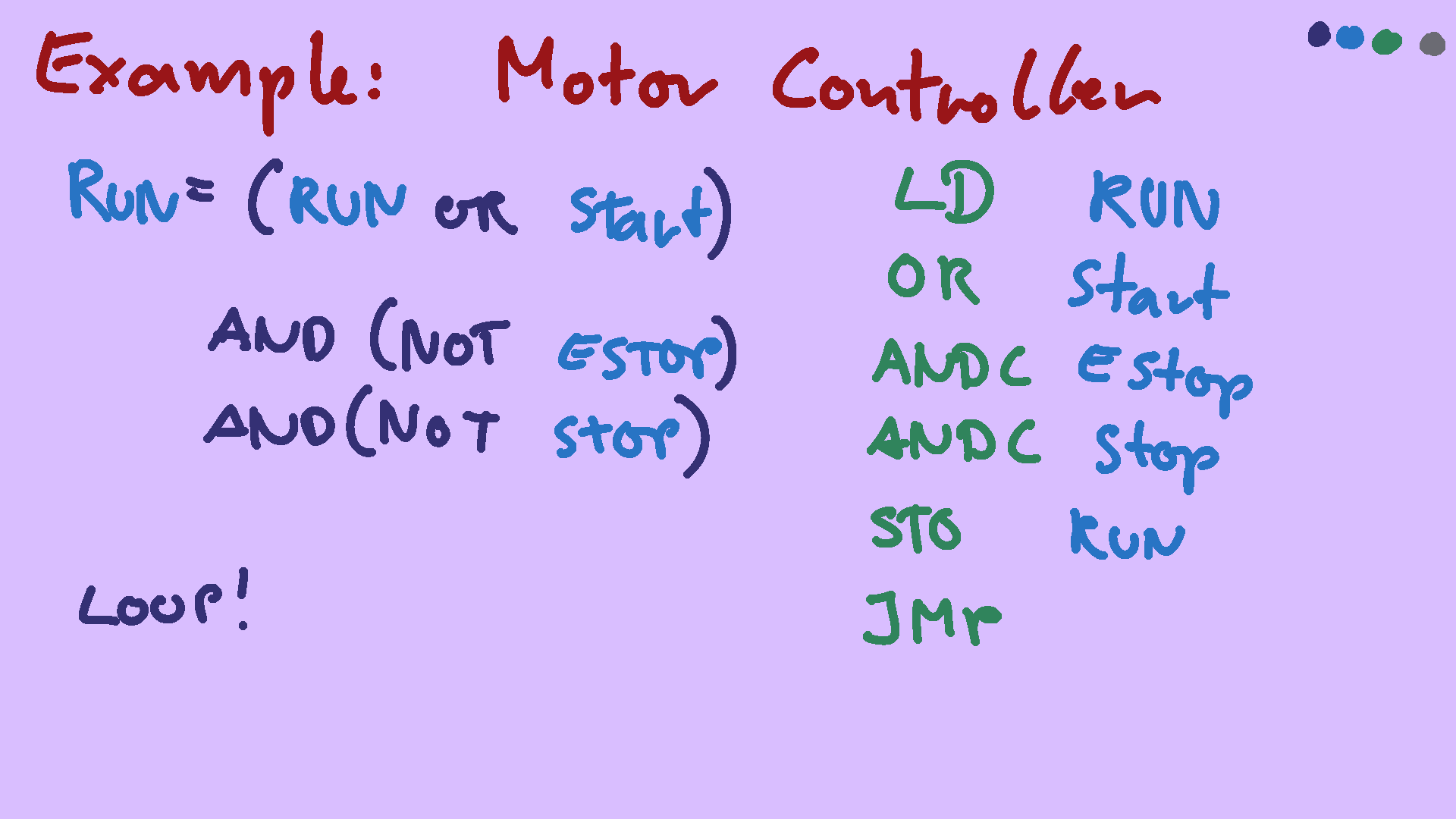
So let's translate it to ICU assembly:
The first section of every MC14500 program is CPU initialization. When the CPU powers up, both input and output are disabled. So we have to use the OR-Complement Result-Register with itself Trick to load a one, and use that to enable everything. You might wonder about the NOP at the beginning: This is needed, assuming you hooked the ReTurN instruction slash output pin up so that it resets the program counter. The instruction immediately following RTN is skipped - skipping the NOP is safe, skipping the ORC isn't.
And that's it. all we need to do is loop back to the beginning.
Congratulations - if you get bored of your COBOL job, you are now qualfiied to switch careers and start programming industrial machinery.
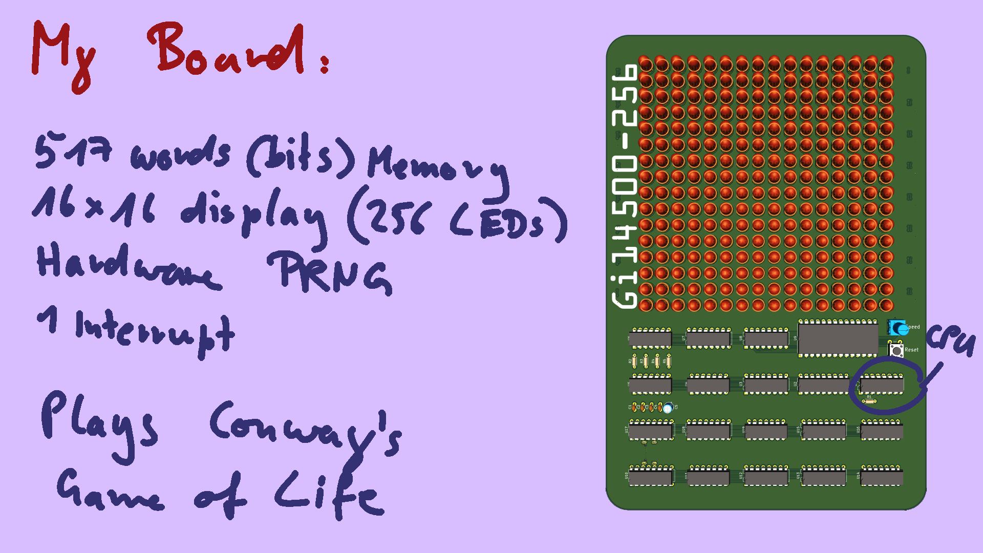
Let's switch gears, and talk about the thing I built. I claim this is the most powerful 14500 project to date: it has 517 words of memory, a 16x16 double-buffered display, a hardware random number generator, and even has an interrupt of sorts. I call it the GI-14500. The 256 suffix is the number of LEDs on the board.
Its purpose is to simply look nice, so I made it play Conway's Game of Life. The Game of Life is not a game you interact with, it's a simulation. Relevant for this talk is only that it makes the LEDs blink in nice patterns.
The computer part is completely period-correct for something that could have existed in the late seventies, early eighties. I've only cheated with putting modern LED driver chips on the back, for purely aestetic reasons. Oh, and I thought it would be hilarious if this obsolete-from-the-start thing was powered over USB-C, so of course I made it fully compliant to the USB-C power delivery spec.
The computer is made up of four subsystems, or peripherals. Let's walk though them.
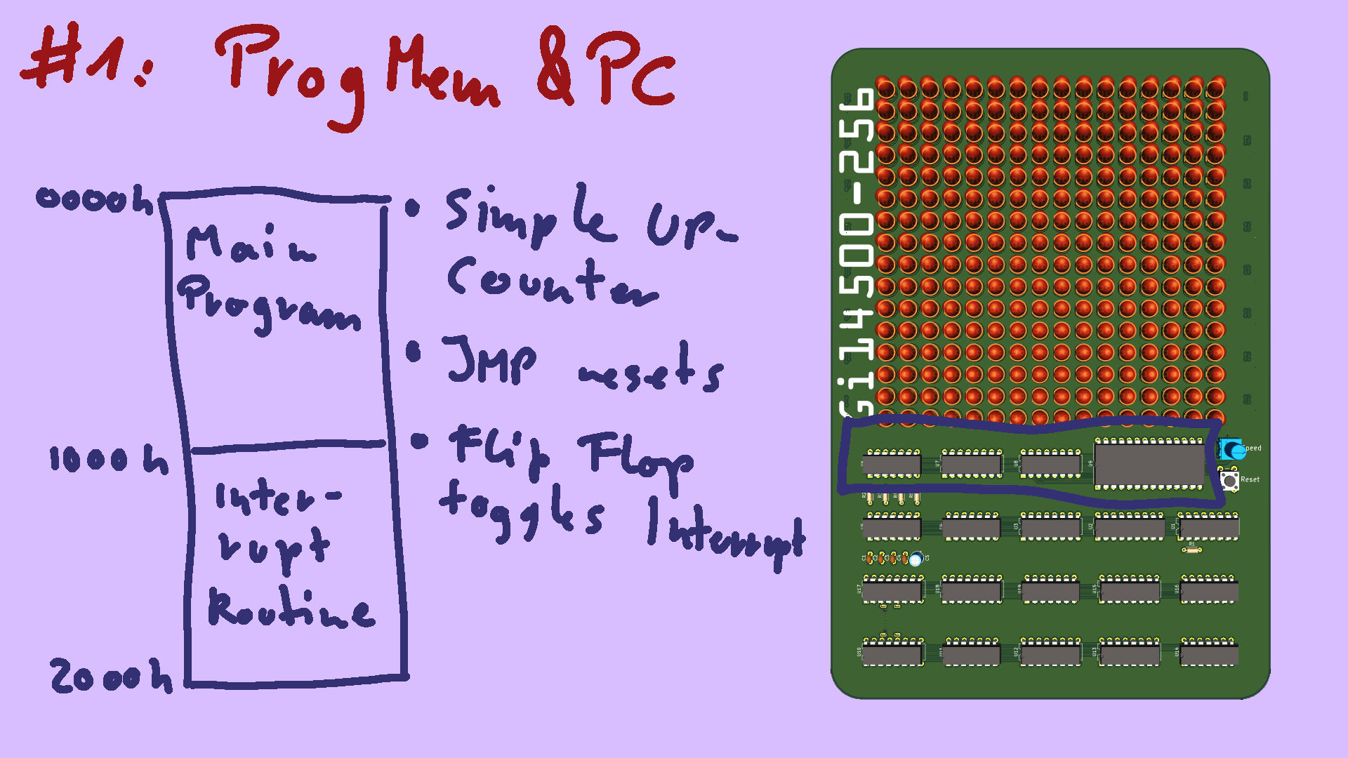
The first is the program memory and program counter unit. It's made up of a simply binary counter, directly attached to the lower half of EEPROM storing our machine code. The upper half of program memory is reserved for the interrupt routine. if this flip-flop is triggered, it simply swiches out the normal program for the interrupt routine, and vice versa. As with the minimal ICU system, JUMP simply resets the counter to zero, looping the program back to the beginning. the RETURN instruction additionally clears the flip-flop, returning from the interrupt, and starting the main program again.
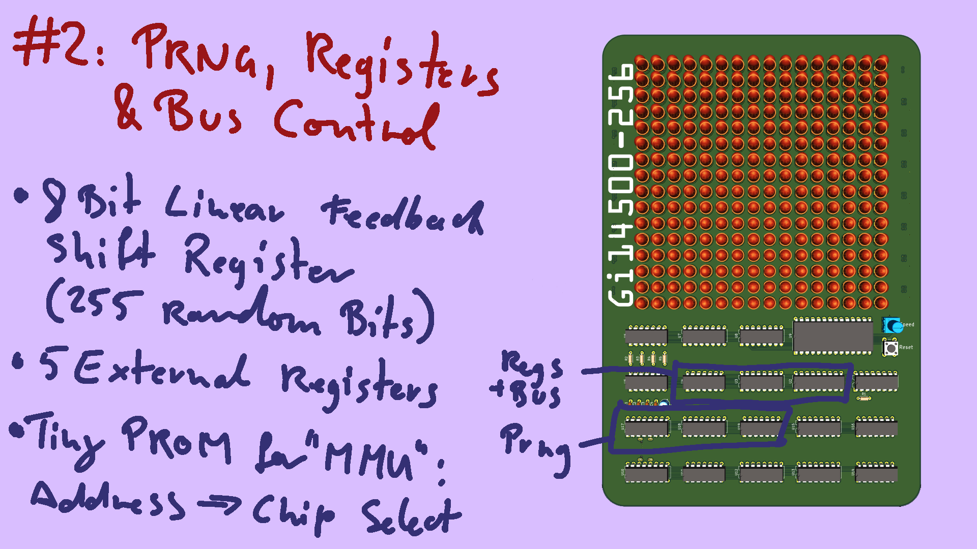
The second subsystem is the register bank and random number generator. Why do we need random numbers? well, this thing is supposed to live on a shelf, blinking away on it's own. It needs some kind of input, and I certainly won't be sitting down with it and punching in hundreds of ones and zeros to make it blink nice. It doesn't generate true randomness, it's only pseudo-random. It's based on a linear feedback shift register and some exclusive-nor gates - that's very easy to implement with minimal components. But it gives nice enough results for what I need. Since the 14500 doesn't have any places to put variables built-in, Motorola came up with a really cool 8-bit latch, the 14599, that is meant to provide eight external registers. My GI14500 only has five of them hooked up, that's all the address space I could spare for it.
There needs to be some logic that determines which of the subsystems should be active, given the current address. This task is handled by a tiny ROM chip, that reads the address lines, and generates an appropriate Chip Select.
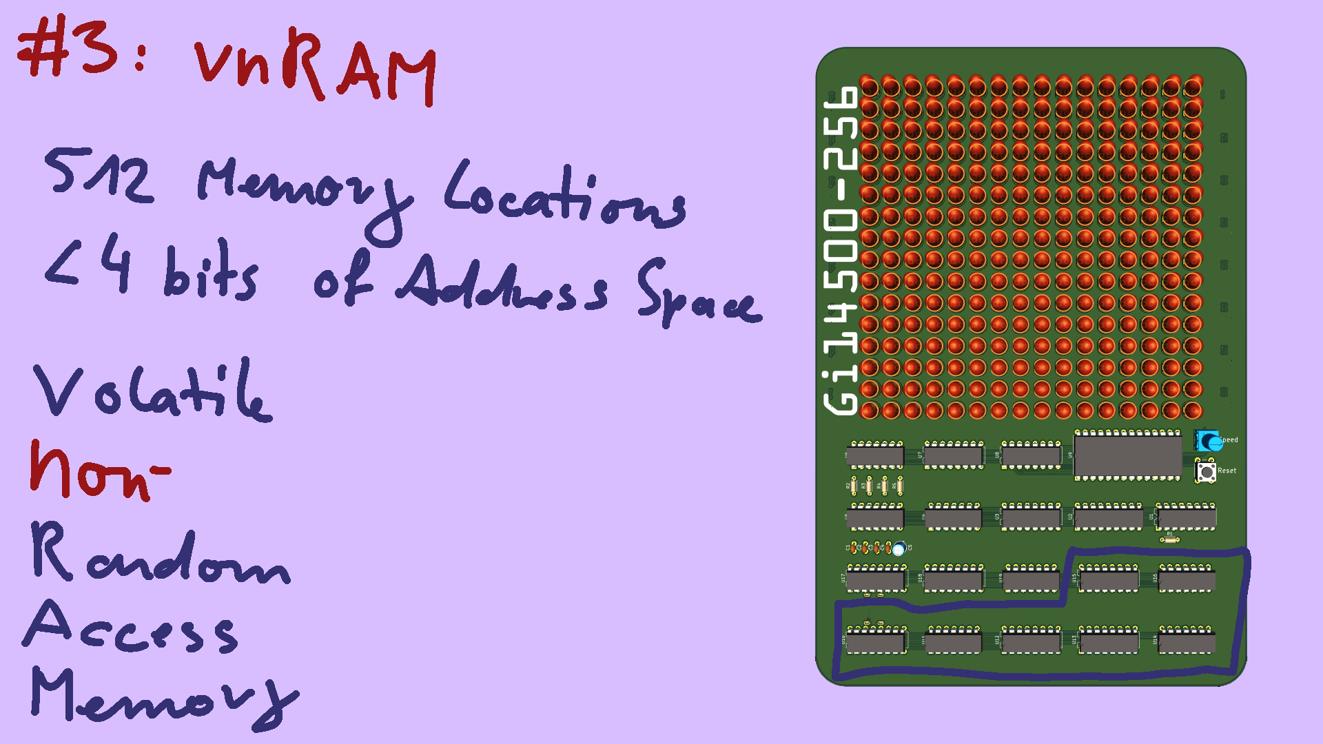
Now let's talk about the main attraction: the 512 bits of memory. As teased in the abstract, I only have 4-bits of address space - that's 16 different memory addresses in total. And we already used up seven of them for the result register, random number generator and registre bank. So how can I access two-to-the-power-of-nine bits of memory, with less than four addressl ines? well, i promosed I'll tell you: it's memory, but it's not randomly accessible - RAM - memory. I'm calling it vnRAM - volatile non-randomly accessible memory. It's a pun of nvRAM, which is RAM that retains its contents after the power is turned off. The basic idea is pretty simple: the address lines of an ordinary RAM chip are not hooked up to the CPU, but to a binary counter, like the program counter, but for RAM. This counter is incremented only when the CPU tells it to - using one of the NOP FLAG output pins of the 14500. This way, we can step through all 512 bits of memory, and when we want to read the next value, strobe the FLAG pin to increment the counter.
But the Game of Life requires us to also look at the surrounding cells to calculate the next state. So we need to be able to temporarily modify the counter value, add plus/minus 1 to look left and right, and plus/minus 16 to look up and down. or both at the same time.
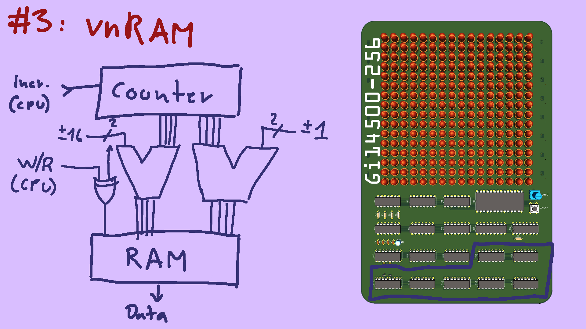
For this, the actual address lines are connected to a pair of full adder chips. Memory location zero simply passes through unmodified and returns the memory cell indicated by the counter. But by asking for other memory addresses, we can change the input of the adders and access the neighbouring fields. There's one more trick: when the CPU writes to memory using the STOre instruction, it puts a signal out on the Write pin. This is nothing special - all CPUs do that - it's necessary so the memory knows that it needs to store the value presented, instead of returning what's already there. But we can make use of this, to invert one of the address lines of the RAM chip. This means whenever one page of memory is opened for reading, writes go to the other. This gives us double-buffering for the cost of just a single XOR gate! pretty neat. With this setup, you could actually implement any graphics filter that uses a 3x3 kernel (well, at a measly bit-depth of 1, so no grayscale, just black or white). The schematic I've put up on screen is of course a simplification. There are some additional gates needed to make subtraction work, or so that reading a non-existent neighbour on the edge of the screen doesn't result in garbage data. But ... details.
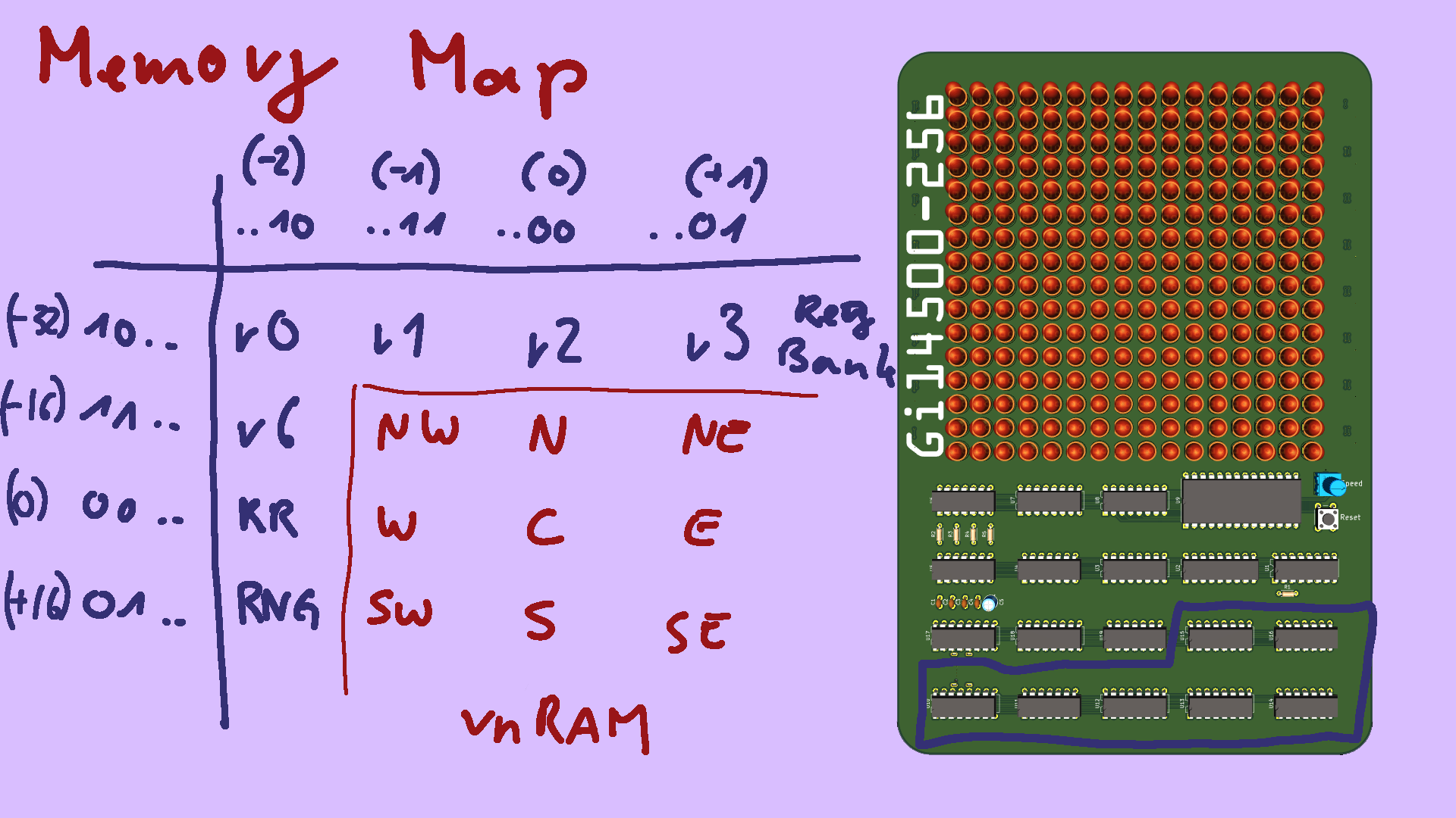
So this is the resulting memory map.
For the vnRAM, we interpret the lower and upper two bits of the address as signed integers, from negative two to plus 1. This is the value added or subtracted from the memory counter.
All the other peripherals are then arranged in the minus 32 and minus two offsets, which the vnRAM unit doesn't need. For example, here's the register bank, there's the result register, and here is the random number generator.
OK, so we have used up all our memory addresses, but we haven't taken the LED matrix display into account. Here's the neat thing: it doesn't require any addresses at all! On the bottom of the board are sixteen 16-bit shift registers, one for each row of the display. Whenever a value gets written to RAM, it is also fed directly into this long shift register - each step of which is hooked up to one of the 256 LEDs. And once all 256 LEDs have been updated, the new state is latched in and displayed.
I won't go into detail on the code - you can read up on it after the talk if you really care. But let's do a quick high-level peek. There are two "modes": simulate and generate. Simulate is the main program, it generates one pixel of the next generation of the board, then loops. Once a full board has been generated, the interrupt fires and displays it. We keep track of whether the board has stopped changing, and the interrupt is also responsible for detecting that, and swithcing to the "generate" mode. The generator then uses the random number generator to create a new board to work on, preventing the display from getting boring. The main simulator program is fairly simple: loop through all neighbours, and count them up. Then, decide if the pixel should turn on or off in the next frame. Then it increments to the next memory address, and loops back to the start. Since we don't have the luxury of arbitrary jumps, the internal loop that checks all the neighbours must be unrolled. I am acutally generating the final machine code with a simply pyhton script as a make-shift assembler: that takes care of unrolling and translating mnemonics and labels to instructions and addresses. That's fed through a series of shell pipelines, until we get a binary file that can be written straight to the EEPROM.
Finally, I thought it would be interesting to look at some of the silly mistakes I've made while building this thing. Since the board contains nineteen chips, excluding the display shift register, I thought it would be a good idea to bring it up in stages. I still think this was the right move, but it caused some troubles. Be really careful that you have tied all your unconnected inputs to ground or 5volts. I knew about this problem, but forgot about a few signals.